
AMZ Buffer Module© 2015,2016 Jack Orman
The circuit is a single class A buffer stage based on a jfet transistor. It has a genuine Fairchild 2N5457 transistor that gives close to unity gain or 0db (gain=1). It is simple to hook up with only 4 wires needed in the basic configuration. Power supply protection and filtering has been provided on board as well as RF blocking on the input. The input impedance is close to 1M (>933k) without the optional pulldown resistor. Low end response easily covers the bass guitar range too. Current requirements are low (less than 1 ma.) and a battery will last a long time. A fresh alkaline 9v is recommended.
Order the pre-assembled Buffer PCB from the catalog page.
R8 is for an optional pulldown resistor, and is used to help prevent pops if the buffer is wired to a bypass switch. A 2.2M resistor with 1/8w rating is recommended. If you are not using a bypass footswitch, do not add R8.
The buffer board can be powered by 18v if required, with no changes needed.
6 Examples Uses for the Buffer Board
1. Standalone BufferThis is one of the most common uses. The buffer is installed in a small box that can be placed anywhere that it is needed on the pedalboard. This is the most flexible configuration. The buffer will mount easily in a tiny 1590A box along with the LED, input, output and power jacks.
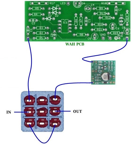
2. Buffer the input of a wah or fuzz
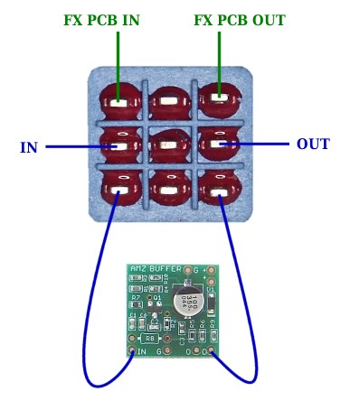
The AMZ pre-assembled buffer module is small enough that it can conveniently fit into a small corner inside the pedal. Use only one of the output pads (do not parallel them) so that the build-out resistance of the buffer is high enough to prevent unwanted interactions with the wah or fuzz. Power and ground connections to the buffer are required but not shown in this wiring diagram.
Used in this manner, the pedal is still true bypass since the buffer is only active when the effect is switched on. (LED wiring on the switch is not shown.)
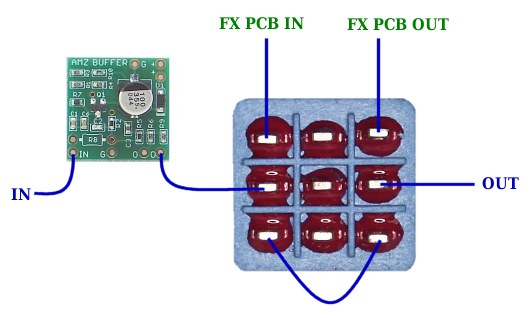
3. Buffer the wah/fuzz output
The buffer module can be used to isolate the problem pedal from the boxes that follow it. In this position, it can also serve as a buffer to isolate a large value output volume pot from the next pedal in line. This prevents interactions that can have an adverse effect on tone. Many fuzzface pedals have a 500k volume pot on their output and the buffer would serve to isolate it and reduce the loading effects (i.e. provide a constant load to the fuzzface). Power and ground connections to the buffer are required but not shown in this wiring diagram.
Used in this manner, the pedal is still true bypass since the buffer is only active when the effect is switched on. (LED wiring on the switch is not shown.)
4. Convert True Bypass to Buffered Bypass
Because the buffer is serving a double function, this is one of the most common mods for pedals. Power and ground connections to the buffer are required but not shown in this wiring diagram.
Used in this manner, the pedal output is now buffered and it is no longer true bypass. R8 is not required. (LED wiring on the switch is not shown.)
5. Loop Bypass
This allows one pedal to have a dual function. The effect circuit (pcb) drives the signal chain when it is active, but the buffer drives the signal path when the effect is bypassed. Since the effect pcb is isolated from the buffer, it performs as it always has, but when the footswitch is toggled, the pedal becomes a standalone buffer. Power and ground connections to the buffer are required but not shown in this wiring diagram.
R8 might be required. LED wiring on the switch is not shown.
Extra Connections
There are also two output signal pads located in the lower right corner. They can be used several ways. Either one can be used alone as the audio output. They both can be used separately to provide isolated outputs for different audio paths. Lastly, the two pads can be jumpered together, which will halve the output impedance of the buffer.
There are also two Ground pads. They are both directly connected to the ground plane on the back of the pcb. There is no difference in them and you can use either or both as required.
More Uses and Ordering Info
Another use would be as a conditioning input for projects that are not designed for use with guitars, and which might have low impedance inputs. Class D amp modules would be an example, or even microprocessor analog inputs. The board isn't much larger than a postage stamp and can be mounted to the side of the enclosure with double sided tape or sticky pads. It could even be stuck to the side of the 3PDT footswitch to keep it out of the way.
Order the pre-assembled Buffer PCB from the catalog page.
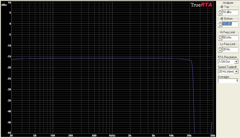
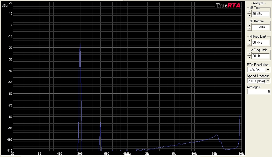
Frequency Response and Distortion I measured the frequency response of this jfet buffer module and it is +/- 1dB from 30 Hz to 20,000 Hz. This easily covers the full range of both the guitar and bass spectrums. A look at the harmonics produced by the module shows that it is very clean. The only harmonic of any prominence is the second (at 400 Hz) and it is well below the fundamental 200 Hz audio, which demonstrates that the module is quite clean (low distortion). The measurements were made when powered by a 9v power supply.
Order the pre-assembled Buffer PCB from the catalog page.
|
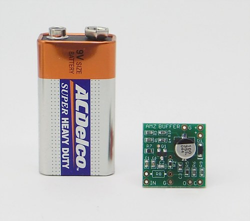 This is a pre-assembled jfet buffer. It has a clean, transparent sound and can be used in numerous ways on your pedalboard or even used to mod existing effect pedals. As can be seen in the photo, the board is very small and not as wide as a 9v battery.
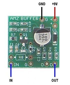 The 8-sided pads on the pcb are for wires to connect to the external parts. The input pad at the bottom left is for the signal from the input jack or footswitch. There are two output pads near the bottom right of the pcb and they can be used individually, or connected together for lower output impedance. The ground connection (Gnd) should be wired to the power jack ground or connected to the ground lug on either the input or output jack. Though 2 ground pads are provided, only one is required for basic operation.
 Another common use would be to install the buffer inside a wah or fuzz pedal as shown here. Many of these pedals have low impedance input and the buffer will convert the input to high impedance and extend the range of frequency response.
 Sometimes a wah or fuzz pedal will have problems with interactions with other pedals that follow them in the signal chain.
 This method is similar to the Boss use of buffers in their pedals. The input to the effect pcb is buffered and the the bypass is also buffered, since the buffer pcb is always in the signal chain.
 I have never seen this connection in a pedal but it is interesting nonetheless. The buffer is inserted in the true bypass loop and converts the pedal to buffered bypass. The interesting feature is that the bypass is buffered but the pedal input is not.
 There are two +9v pads included for convenience. They are jumpered together on the pcb and there is no difference between them. You can use either one or both. An example use for the second pad would be to provide power for an LED.
 Since the buffer board is tiny and requires little power, it can be retrofitted into almost any existing pedal to provide proper interfacing with guitars, basses, and oher pedals.
AMZ-FX Home Page
Lab Notebook Main Page
Guitar Effects Blog
©2015 Jack Orman
All Rights Reserved