
|
Tutorial: Making a Groundplane using Cadsoft Eagle
If you decide to make this for use with your guitar, and intend to leave it in the circuit at all times to provide a buffered signal, then I suggest that you leave out R1 as it will not be needed.
The values shown here will give good performance but can be tweaked to suit your taste. For example, if it is a bit too bright for your rig, reduce the values of both R2 and R3 to 1M, or even 470k to see if the lower input impedance takes some of the edge off.
The jfet transistor Q1 can be any common small signal device such as the 2N5457, MPF102, or J201.
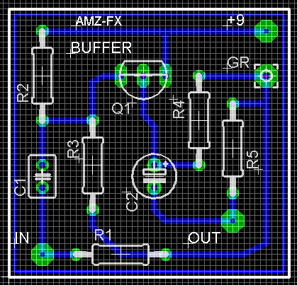
This board is about 1.25" square and will easily fit in a small enclosure. You should be able to visualize the positioning of each component as it is related to the schematic above. A complete archive that includes the schematic and the board in Eagle format is available at the end of this article for download. Open the pc board file in Eagle to try the method shown in this article to create the groundplane. It should look exactly like the image shown here on the left.
There are two pads for connecting wires in the upper right corner of the board. The top one is for the positive 9v battery connection and below it is the ground pad, which has white layout corners around it. The blue traces that lead away from the pad are all ground points for components on the board.
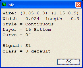
Note that the ground trace is named "S1". If you click on any of the other blue wire elements that connect to the ground pad, you will see that they all are also named "S1". We can change the name of the ground system if we like. On the top menu bar, select "Edit" then "Name" from the dropdown list. Click on the blue trace below the GR label and a box will popup that allows the name of the element to be changed. Delete the S1 label and type in GND and hit the OK button. The ground traces are now all named GND and that can be verified by using the View/Info function as we did before.
Before we draw the polygon, a couple of the default values need to be changed. The width of the line should be changed to 0.010. The Isolate value, which is how much space will be between the groundplace polygon and the other non-grounded elements needs to be selected. On the current version of Eagle it defaults to 0 which is not useful. I select 0.016 or sometimes 0.024 for the Isolate value.
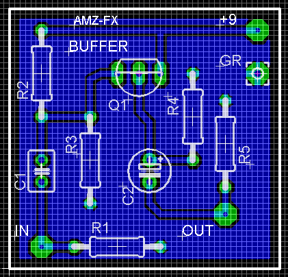
The polygon is the blue box just inside the white border of the pcb. To make the groundplane, we rename the polygon to the same name that is used for the traces connected to the ground pad. If you have changed the name as taught earlier in this article, it will be called GND. To rename the polygon, we go to "Edit" on the top menu, then "Name" from the dropdown list. Now click on the blue polygon line and the box will popup that allows you to enter a new name for the polygon, which we will enter as GND.
If the groundplane does not appear, click the Ratsnest button on the sidebar. Should it still not appear, you likely do not have the polygon and the ground traces using the same name. Did you rename "S1" as instructed in an earlier paragraph? Note that the pads for all of the components that were connected to ground are now isolated but tied to the groundplane with short copper traces. The components that are not grounded are isolated electrically from the groundplane by a clear space around each pad and trace, which will be the width that was selected in the "Isolate" menu item.
This type of copper pour is also used to create small heatsink pads on the pcb for transistors or voltage regulators.
A small board like this one, especially one with low gain, probably does not improve much by having a groundplane but there is one advantage. By pouring a copper fill on the bottom of the board, less copper has to be removed when the board is etched and this extends the life of your ferric chlroide etchant making it capable of doing more boards before it is depleted. I hope this short tutorial helps you with your Eagle CAD layouts, and the jfet buffer may be a useful additional to your guitar effects pedalboard. Notes:
Download: PCB layout and schematic PDF version of this tutorial: Groundplane.pdf (133k) If you need a buffer but do not want to go to the trouble to make your own pc board, this buffer can be built on the AMZ Multi-Purpose pcb.
|
|
AMZ-FX Home Page
Lab Notebook Main Page
Guitar Effects Blog
©2007 Jack Orman
All Rights Reserved
 This is the schematic of the simple jfet buffer that will be used in this tutorial. It is a fully functional circuit that is ready for use on an effects pedalboard. It is one of the circuits from the
  This is what the printed circuit layout looks like when the schematic has been entered into Cadsoft's Eagle Layout Editor. The free version of Eagle is sufficient for most stompbox circuits and is an excellent editor for pc boards, though it can be a bit challenging at first.
 Let's view the info about the ground traces. Go to the top menu bar in Eagle and select "View", then "Info" from the dropdown list. Now if you click on the blue ground trace below the label GR on the pc board, a box will pop up with the info about that circuit element. The info should be as shown in this example.
 Finally we are to the actual creation of the groundplace itself. This is done by using the Polygon tool in Eagle. Click on the Polygon button and a new menu will popup directly above the pc board layout. This is the parameters that will be used for the polygon that will be drawn on the board. Make sure that the bottom layer is selected, which will be the far left item of the new menu.
 When you have the polygon drawn completely around the perimeter of the circuit, it should look similar to the example here.
 There will be another popup box to confirm that you want to connect the polygon to GND, so select it from the choices and hit the OKAY button. The groundplane should automatically fill the bottom layer of the pcb as shown here. You can hit the F2 key to refresh the view and cleanup any stray bits.
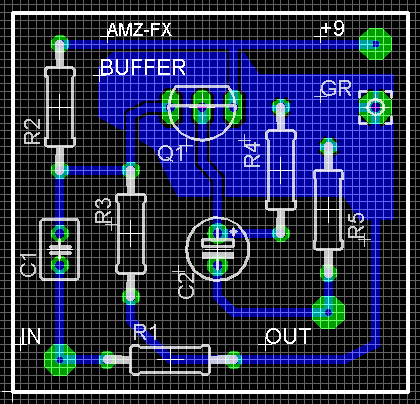
 The groundplane does not have to encompass the entire perimeter of the board nor does it even have to be rectangular. Here I have made a small irregular ground fill that just covers the transistor and a few of the component pads. It is not typically done this way on small boards but on larger, more complex layouts this may come in handy.