
Dual Buffer PC BoardCUSTOMIZED AMP STYLE INPUT
BASIC PC BOARD
Only one buffer can be constructed on the pcb so you must chose whether to use the transistor or opamp version. Both versions have the amp-like input but the opamp version is capable of giving lower output impedance (Z) and unity gain (gain=1), whereas the jfet's output will be higher impedance and slightly less than unity.
The jfet has the advantage of using less current.
Neither version uses all of the parts that are shown on the pcb, so any components that are not in the parts list will not be used, and their place on the pcb is left empty. A jumper is always required on the J1 pads so remember to check the instructions for the type buffer you have chosen to build.
JFET TRANSISTOR BUFFER R1 is a pulldown resistor. It is only used if you are going to use a footswitch to turn the buffer on/off. If you intend to leave the buffer on at all times, then R1 is not required and it should be left out.
Parts List
R1 - 2.2M
All resistors are 1/4w and capacitors are in uF, except for C2.
OPAMP BUFFER R1 is a pulldown resistor. It is only used if you are going to use a footswitch to turn the buffer on/off. If you intend to leave the buffer on at all times, then R1 is not required and it should be left out.
Parts List
R1 - 2.2M
All resistors are 1/4w and capacitors are in uF, except for C2.
BUFFER FOR PIEZO PICKUPS Piezo pickups need a very high input impedance so R2 is increased to 10M ohms. The low pass filter is eliminated in this example by reducing the value of R3 and not using C2. If the piezo produces a strong output signal, it may be necessary to power the buffer with 12v, 15v or even 18v so that the buffered output is undistorted on the loudest notes.
Parts List
R1 - not used
All resistors are 1/4w and capacitors are in uF. The R1 pulldown resistor is not needed when connected to the pickup at all times.
KLON-LIKE OPAMP BUFFER This is not an exact duplicate of the Klon buffer since the parts are positioned slightly differently. Even so, the performance should be the same. R1 is a pulldown resistor. It is only used if you are going to use a footswitch to turn the buffer on/off. If you intend to leave the buffer on at all times, then R1 is not required and it should be left out. The Klon pedal did not have a pulldown on the input.
Parts List
R1 - 2.2M All resistors are 1/4w and capacitors are in uF, except for C2.
NOTE: The value of C4 is the same as in the original pedal but it does not have to be that high in capacitance. A 10uF for C4 will perform just as well, and will be smaller and cheaper.
MODIFICATIONS NOTES:
The Ground pad (marked with a G) should have a wire connecting it with a common ground point inside the pedal, usually the ground lug on either the input or output jack. The +9v pad can be wired to the battery positive (usually the red wire) or to the voltage lug on the dc power jack, if you are using an external power supply. A stereo jack on the input can be used to switch the ground connection from the battery. The battery negative (black wire) is connected to the ring connection on the stereo jack, which is the middle body section on the jack. When a mono plug is inserted into this stereo jack, it makes a connection with the sleeve of the plug, which is also connected to ground, and this makes the connection that turns on the power to the pedal. The C2 layout is a little unusual since it has 3 pads. The top two pads of C2 are actually connected together. This allows a large capacitor to be used on the top to bottom pads (middle empty) without having to bend the leads of the capacitor. This is done to accomodate mica capacitors which are usually large in size. If a small ceramic capacitor is used for C2, then it is placed on the bottom 2 pads of the C2 layout and the top pad is left empty.
OUTPUT IMPEDANCE The value of R5 essentially determines the output impedance. Its value may be increased if desired. One reason to make it higher is to make the buffer more compatible with a fuzz pedal that you have placed after the buffer. A 1k value for R5 is a good starting point but it can be made higher, even 5k or 10k. The values shown on the parts list are best for low impedance line driving and should not be changed unless there is a good reason to do so. OTHER TRANSISTORS The Q1 jfet transistor can be most any common device. Other suitable jfets are the 2N5484, MPF102 and the 2N3819. You won't hear much difference in the various transistors, and I usually select one with low noise characteristics. 18 VOLT POWER
Any version of the buffer pcb can be powered with 12v or even 18v for more clean headroom. I usually use 18v on my pedalboard.
OTHER OPAMPS
The IC1 opamp can be most any dual opamp chip. The 4558, 4559, 5532 or many others can be used with this pcb. In my experience, the LM4562 is the ultimate for low noise and minimal distortion, but it does not always perform as expected. See my blog posts about the LM4562 before using it.
MOUNTING HOLE
CIRCUIT SELECTION
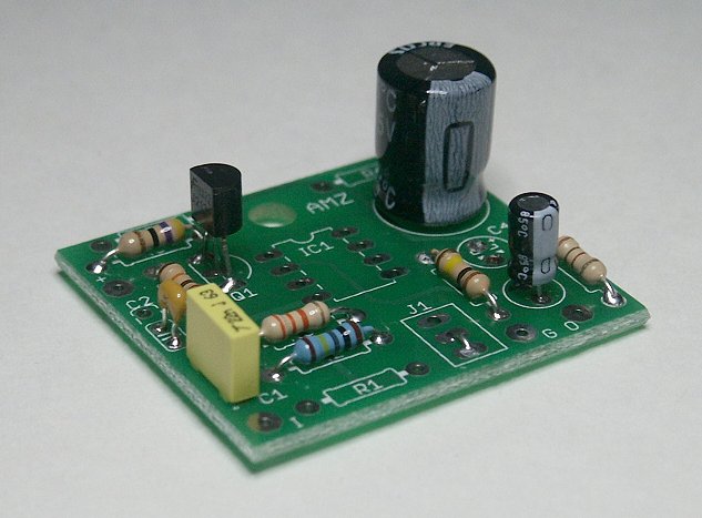
For use at the end as a line driver, I will go with the opamp version. They both sound great and the choice is up to you. My jfet buffer shown in this picture does not have the R1 pulldown resistor as it will be left on all the time. R2 is a metal film 1M resistor for better noise performance. Note the jumper on the bottom two pads of J1.
|
 This pcb has been designed to be only a buffer board, and it can be constructed using a jfet transistor or a dual opamp as the active device. What makes the board special is that the input has been designed to duplicate the input circuitry of the typical tube amp, and it thereby preserves the interaction between the guitar's pickups and the buffer circuit. This makes the sound of the guitar more natural, with a similar resonant peak, while still providing a low impedance output drive for your cables and pedalboard.
 A small jumper wire is soldered on the bottom two pads of the J1 jumper. The top pad has no connection with the transistor buffer.
 A small jumper wire is soldered on the top two pads of the J1 jumper. The bottom pad has no connection with the opamp buffer.
 Every buffer built on this pcb requires a jumper to be set on the J1 pads. The pads to use are noted in the instructions above for each type of buffer so make sure to solder the jumper in place on the board. The jumper in the picture to the left is on the bottom 2 pads of J1.
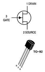 The jfet layout is configured for the common 2Nxxxx pin designation, which is D-S-G, looking at the flat side of the transistor with the pins going down. If a BF245 or 2SK170 or other alternate jfet is used, then the pin configuration may be different and will require orienting the transistor differently to make the proper connections. Check the datasheet for the transistor that you are using.
 There is a hole in the pcb above the IC1 pads and it is sized to accept a common type mounting clip, such as the LAD187, which is available most parts suppliers, such as Mouser or Small Bear Electronics. The LAD187 fits through the hole in the pcb and its bottom side has an adhesive pad that sticks to the enclosure and holds the board in place (shown here on a Multi-Purpose pcb).
 I usually select the jfet buffer if I am going to use it at the input of a pedalbord.
|
A single pc board is $10.00 US plus shipping I prefer Paypal payments. | Place your order on the catalog page. |
More Circuits for this pcb.
AMZ-FX Home Page
Lab Notebook Main Page
Guitar Effects Blog
©2016 Jack Orman
All Rights Reserved